E-Beam Wafer Inspection System Market
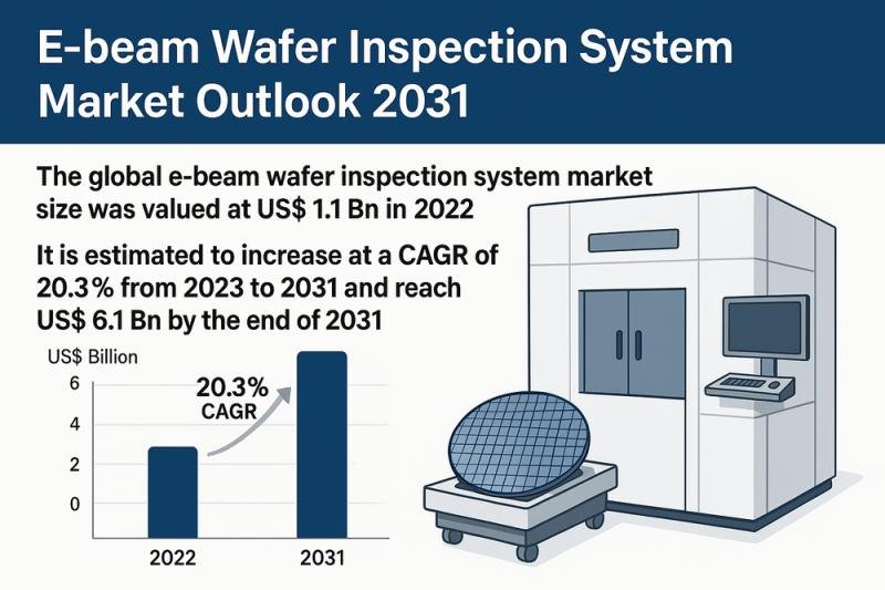
According to recent market research, the global e-beam wafer inspection system market was valued at USD 1.1 Bn in 2022 and is projected to surge to USD 6.1 Bn by 2031, expanding at a robust CAGR of 20.3% from 2023 to 2031. This significant growth is driven by ongoing advancements in semiconductor manufacturing, particularly the shrinking of semiconductor nodes and the rising adoption of advanced packaging technologies.
Download to explore critical insights from our Report in this sample – https://www.transparencymarketresearch.com/sample/sample.php?flag=S&rep_id=15884
Market Overview
E-beam wafer inspection systems are pivotal in modern semiconductor fabrication processes, leveraging high-energy electron beams to examine wafers for defects at extremely high resolutions. These systems provide the detailed insights necessary to maintain the integrity of complex semiconductor devices, including logic and memory chips, during and after the production process.
The increasing miniaturization of semiconductor components and the shift toward advanced technology nodes have elevated the demand for inspection tools that can detect defects invisible to conventional optical systems. The e-beam wafer inspection system market is thus becoming essential for quality control and yield optimization in semiconductor manufacturing.
Market Drivers & Trends
A key driver of market expansion is the adoption of Extreme Ultraviolet (EUV) lithography, which supports the development of next-generation chips at nodes below 10nm. The increasing complexity of integrated circuits, due to multi-layer stacking in 2.5D and 3D architectures, also necessitates high-resolution, high-throughput inspection tools.
One of the latest trends shaping the industry is the development of multi-beam inspection systems. These systems deliver significantly improved throughput and enable the detection of minute defects that are undetectable using traditional single-beam tools. As semiconductors become smaller and more complex, these multi-beam systems offer the scale and speed required for industrial-scale production.
Key Players and Industry Leaders
Several major industry players are leading innovation in this market, including:
Applied Materials Inc.
ASML Holding N.V.
Hitachi Ltd.
HOLON Co., Ltd.
KLA Corporation
MKS Instruments, Inc.
PDF Solutions
Photo electron Soul Inc.
TASMIT, Inc.
Telemark Factory
ZEISS Semiconductor Manufacturing Technology
These companies are focused on improving electron optical systems, enhancing data processing capabilities, and offering advanced analytics that facilitate defect detection and faster decision-making in semiconductor fabrication lines.
Recent Developments
Innovation remains central to competitive strategy in this market:
Hitachi introduced the GS1000 e-beam inspection system designed for EUV 3nm and 5nm processes. It combines high-resolution imaging with rapid data processing, tailored to meet the defect detection demands of cutting-edge semiconductor nodes.
KLA Corporation launched the eSL10TM e-beam defect inspection technology in 2020, aimed at reducing inspection times and improving yields for advanced memory and logic chips. The platform is especially effective for detecting anomalies in EUV-patterned wafers.
Latest Market Trends
The shift toward multi-beam inspection is the most notable trend, driven by the need for faster, more efficient analysis at scale. Traditional single-beam systems face throughput limitations that make them less suitable for high-volume manufacturing. Multi-beam technology is now becoming a cornerstone for semiconductor fabs aiming to maintain pace with innovation while ensuring yield optimization.
Additionally, the rise in automated defect classification and AI-powered analytics in e-beam systems is enhancing their role in predictive maintenance and process improvement, providing fab operators with better insights and faster root cause analysis.
Market Opportunities
Opportunities abound in the areas of:
Advanced nodes (7nm and below) where inspection precision is critical
2.5D and 3D packaging technologies, which demand defect detection across multiple layers and interfaces
AI-integrated inspection platforms offering real-time analysis and feedback loops for yield improvement
Furthermore, emerging markets in automotive electronics, healthcare devices, and IoT present untapped demand for semiconductor components, thus requiring inspection technologies to ensure quality and reliability at high volumes.
Future Outlook
Looking ahead, the e-beam wafer inspection system market will continue to grow rapidly as semiconductor technologies evolve toward smaller nodes and more complex structures. The deployment of 5G, AI, and autonomous vehicles will further drive the need for defect-free chips with high reliability.
Analysts forecast a growing preference for multi-beam systems, AI-enhanced analytics, and integration with smart manufacturing platforms. Vendors investing in R&D and strategic partnerships will be best positioned to capitalize on this market’s exponential growth potential.
Buy this Premium Research Report to stay ahead with cutting-edge data – https://www.transparencymarketresearch.com/checkout.php?rep_id=15884
About Transparency Market Research
Transparency Market Research, a global market research company registered at Wilmington, Delaware, United States, provides custom research and consulting services. Our exclusive blend of quantitative forecasting and trends analysis provides forward-looking insights for thousands of decision makers. Our experienced team of Analysts, Researchers, and Consultants use proprietary data sources and various tools & techniques to gather and analyses information.
Our data repository is continuously updated and revised by a team of research experts, so that it always reflects the latest trends and information. With a broad research and analysis capability, Transparency Market Research employs rigorous primary and secondary research techniques in developing distinctive data sets and research material for business reports.
Contact:
Transparency Market Research Inc.
CORPORATE HEADQUARTER DOWNTOWN,
1000 N. West Street,
Suite 1200, Wilmington, Delaware 19801 USA
Tel: +1-518-618-1030
USA – Canada Toll Free: 866-552-3453
Website: https://www.transparencymarketresearch.com
Email: sales@transparencymarketresearch.com
This release was published on openPR.