EUV Lithography Market
Market Size and Growth
EUV Lithography Market is expected to grow at CAGR of 12% during the forecast period 2024-2031
Request Executive Sample Report (Get Higher Priority for Corporate Email ID):- https://www.datamintelligence.com/download-sample/euv-lithography-market?kb
United States: Recent Industry Developments
✅ February 2026: Intel unveiled its next-generation EUV lithography process for 3nm and below semiconductor nodes, enhancing transistor density and performance.
✅ January 2026: ASML partnered with U.S.-based chip manufacturers to optimize EUV systems for high-volume production of advanced logic chips.
✅ December 2025: Applied Materials introduced EUV-ready photomask inspection and cleaning solutions to improve yield in advanced fabs.
Japan: Recent Industry Developments
✅ February 2026: Tokyo Electron advanced EUV lithography integration for semiconductor foundries producing 3nm and 2nm chips.
✅ January 2026: Nikon developed high-precision EUV optics to enhance throughput and patterning accuracy for Japanese chipmakers.
✅ December 2025: Japanese semiconductor consortia invested in R&D to adopt EUV technology for automotive and AI chip production.
Industry Collaborations & Partnerships:
NanoFab Reflection EUV Center (U.S.)
✦ A large, $10 billion consortium including ASML, IBM, Applied Materials, Tokyo Electron, New York state, and other partners is investing in a next‐gen lithography R&D hub at Albany NanoTech – a critical strategic investment rather than an outright acquisition.
Research Partnerships
✦ NY Creates and SCREEN (Japanese semiconductor equipment maker) agreed on a 10‐year, $75 million research collaboration tied to High‐NA EUV lithography technology at the Albany NanoTech facility.
Key Players 2026:
ASML, Canon Inc., Intel Corporation, Nikon Corporation, NuFlare Technology Inc., Samsung Corporation, SUSS Microtec AG, Taiwan Semiconductor Manufacturing Company Limited (TSMC), Ultratech Inc., Vistec Semiconductor Systems
Growth Forecast Projections 2026:
The Global EUV Lithography Market is anticipated to rise at a considerable rate during the forecast period, between 2026 and 2033. In 2025, the market is growing at a steady rate, and with the rising adoption of strategies by key players, the market is expected to rise over the projected horizon.
Global / ASML Highlights 2026:
✦ ASML is expanding beyond EUV, exploring AI chip packaging, stacking, and next-gen multi-layer architectures.
✦ The XT:260 scanner targets AI and advanced memory processors; AI-driven control and inspection enhance efficiency.
✦ Third-generation EUV systems and new light-source advances could boost chip output by up to 50% by 2030.
✦ ASML’s $560 B valuation reflects its dominance and nearly 30% stock rise this year.
China EUV Developments
✦ China has produced its own EUV lithography machine with a superior laser-generated plasma source.
✦ The development signals Beijing’s push for semiconductor self-sufficiency.
✦ Local EUV tech aims to compete with ASML in advanced chip production.
✦ Focus includes enhancing resolution and output for domestic high-end logic chips.
Key Market Developments 2026:
✅ February 2026: Semiconductor manufacturers accelerated deployment of EUV systems for 3nm and sub-3nm node production, increasing yield efficiency and reducing defect rates in high-volume chip fabrication.
✅ January 2026: Leading equipment vendors expanded EUV solutions with enhanced light source power, mask defect detection, and multi-patterning capabilities to support advanced logic and memory chip manufacturing.
✅ December 2025: Adoption of EUV lithography accelerated in Asia-Pacific semiconductor fabs, supporting high-volume production of logic chips, DRAM, and NAND flash memory with improved precision and throughput.
✅ November 2025: EUV systems integration enabled faster cycle times and reduced manufacturing complexity by combining advanced process control, real-time overlay correction, and automated patterning.
✅ October 2025: Semiconductor foundries invested in next-generation EUV photoresists and pellicle technologies to improve resolution, contamination control, and process stability for sub-5nm nodes.
✅ August 2025: Chipmakers optimized EUV tool utilization with AI-driven scheduling and predictive maintenance, enhancing operational efficiency and reducing downtime.
✅ June 2025: Rising demand for advanced logic and memory devices fueled early adoption of EUV lithography platforms in emerging semiconductor markets, including India, Taiwan, and Southeast Asia.
Buy Now & Unlock 360° Market Intelligence: https://www.datamintelligence.com/buy-now-page?report=euv-lithography-market?kb
Latest Technology EUV Lithography 2026:
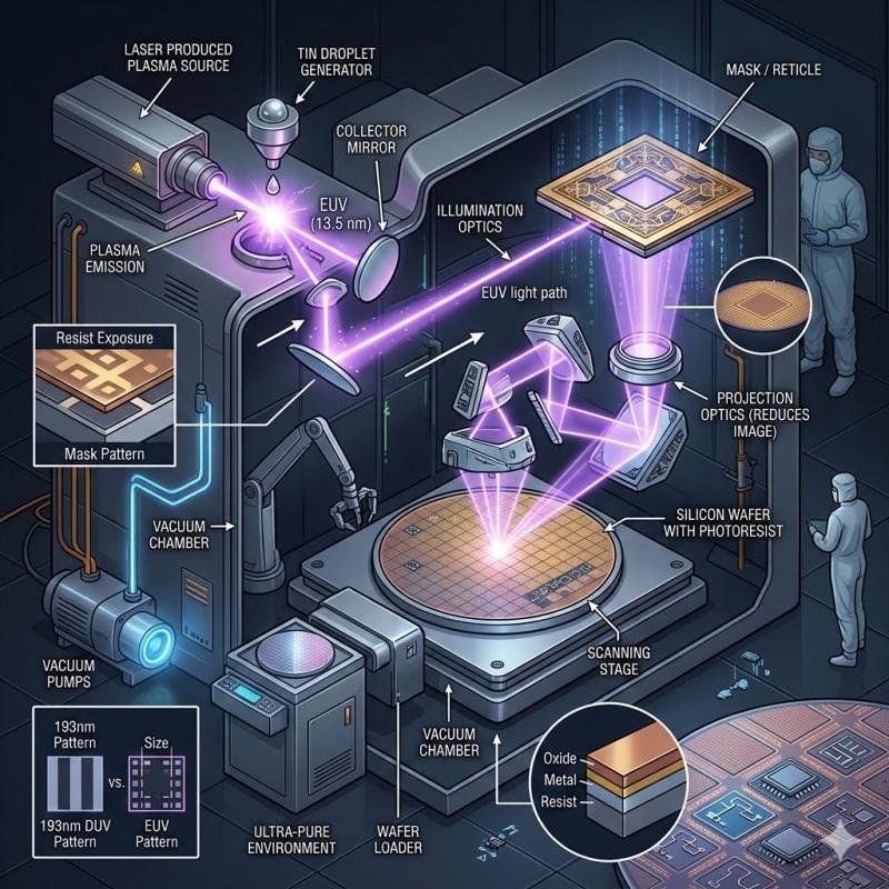
✅ High-NA EUV: Increases numerical aperture for finer patterning below 3nm nodes.
✅ Laser-Produced Plasma (LPP) Sources: Brighter EUV light generation for faster wafer throughput.
✅ Multi-Patterning Integration: Reduces defects and improves layer precision for advanced chips.
✅ Resist & Mask Innovations: Enhanced sensitivity and durability for sub-5nm fabrication.
✅ Throughput Optimization: Advanced scanner optics and pellicles for higher productivity.
✅ AI-Enhanced Process Control: Real-time monitoring and predictive adjustments for yield improvement
Major Regional Growth Share 2026:
✅ North America: 35% – Leading market fueled by semiconductor fabs and cutting-edge chip R&D.
✅ Europe: 20% – Growth supported by EU-based R&D centers and equipment suppliers.
✅ Asia-Pacific (including Japan): 30% – High adoption across China, Taiwan, South Korea, and Japan for advanced chip manufacturing.
✅ Middle East & Africa: 5% – Emerging interest via semiconductor R&D and industrial tech initiatives.
✅ Germany: 4% – Advanced semiconductor R&D and EU-based equipment hubs.
✅ United Kingdom: 3% – Moderate adoption in chip design and specialized manufacturing.
✅ South Korea: included in Asia-Pacific – Key fab sites driving advanced node production.
✅ Canada: 2% – Growing adoption in chip prototyping and R&D centers.
✅ Spain: 1% – Early-stage adoption in semiconductor research projects.
Get Customization in the report as per your requirements: https://datamintelligence.com/customize/euv-lithography-market?kb
Key Segmentations 2026:
By Light Source: Laser Produced Plasma, Vacuum Sparks, Gas Discharges
By Application: Integrated Device Manufacturer, Foundry
By Equipment: Light Source, Mirrors, Masks, Others
Market Growth Drivers
AI & HPC Demand: Chips below 5 nm (soon 2 nm) require EUV for reliable production.
Government Support: U.S., EU, and Asian chip initiatives are fueling EUV tool orders.
High-NA EUV: ASML’s 0.55 NA machines offer 3× better resolution; Intel has the first unit, with TSMC and Samsung next. Each costs $384 M but boosts productivity.
Efficiency Boost: Fewer patterning steps speed production, cut power, and improve performance benefiting Apple, Nvidia, AMD, and other fabless firms.
Unlock 360° Market Intelligence with DataM Subscription Services: https://www.datamintelligence.com/reports-subscription?kb
✅ Competitive Landscape
✅ Sustainability Impact Analysis
✅ KOL / Stakeholder Insights
✅ Unmet Needs & Positioning, Pricing & Market Access Snapshots
✅ Market Volatility & Emerging Risks Analysis
✅ Quarterly Industry Report Updated
✅ Live Market & Pricing Trends
✅ Import-Export Data Monitoring
Contact Us –
Company Name: DataM Intelligence
Contact Person: Sai Kiran
Email: Sai.k@datamintelligence.com
Phone: +1 877 441 4866
Website: https://www.datamintelligence.com
About Us –
DataM Intelligence is a Market Research and Consulting firm that provides end-to-end business solutions to organizations from Research to Consulting. We, at DataM Intelligence, leverage our top trademark trends, insights and developments to emancipate swift and astute solutions to clients like you. We encompass a multitude of syndicate reports and customized reports with a robust methodology.
Our research database features countless statistics and in-depth analyses across a wide range of 6300+ reports in 40+ domains creating business solutions for more than 200+ companies across 50+ countries; catering to the key business research needs that influence the growth trajectory of our vast clientele.
This release was published on openPR.