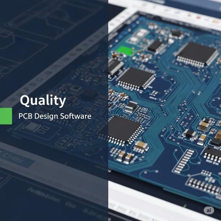
PCB Design Software Market
The Printed Circuit Board (PCB) Design Software Market is poised for a period of transformative growth between 2025 and 2035, fueled by increasing demand for advanced electronics, the rise of AI-driven design optimization, and broader PCB design automation. According to recent projections, the market is set to expand from USD 5.35 billion in 2025 to USD 21.91 billion by 2035, reflecting a robust CAGR of 15.1% over the forecast period.
As the complexity of electronic devices increases and industries embrace IoT, 5G, automotive electronics, and consumer wearables, efficient, intelligent PCB design tools are becoming critical to product development cycles. This rapid shift toward smarter design platforms is revolutionizing the way circuit boards are conceptualized, developed, and validated.
Stay Informed on Key Market Changes: Get a Sample Report! https://www.futuremarketinsights.com/reports/sample/rep-gb-854
Driving Forces Behind Market Growth
• Explosion in High-End Consumer Electronics
The demand for smaller, lighter, and more powerful devices is pushing designers to rely on advanced PCB design tools that support multi-layered, high-density board layouts.
• Integration of AI and Machine Learning
PCB design tools powered by AI are significantly reducing design errors, optimizing routing, and automating repetitive tasks, improving speed and accuracy.
• Shift to PCB Design Automation (EDA Tools)
The transition from manual to automated Electronic Design Automation (EDA) systems is enabling faster prototyping, cost savings, and reduced time-to-market for manufacturers.
• Adoption Across Emerging Industries
Industries such as aerospace, defense, automotive, and medical devices are adopting sophisticated PCB design solutions to meet stringent performance and safety standards.
• Cloud-Based Collaboration & Remote Design
The COVID-19 pandemic accelerated the need for remote-access design tools. Cloud-based PCB software now enables teams to collaborate globally and simultaneously on complex designs.
• Growing Emphasis on Energy Efficiency & Miniaturization
Eco-friendly electronics and the miniaturization of devices require precise, efficient circuit layouts that advanced PCB software tools are well-equipped to provide.
Market Challenges & Strategic Responses
• High Initial Cost of Licensing and Tools
Premium features in PCB design software often come with a steep learning curve and high subscription/licensing costs.
Response: Vendors are offering modular pricing, freemium models, and cloud-based subscription plans to attract smaller firms and startups.
• Skilled Talent Shortage
There is a lack of engineers proficient in handling next-gen PCB software integrated with AI and automation.
Response: Companies are investing in training, certification programs, and user-friendly interfaces to reduce the learning barrier.
• Complexity of Regulatory Compliance
Meeting international safety and functionality standards can slow down innovation.
Response: Software providers are embedding compliance checks and automatic rule-verification features within the design tools.
• Design Reusability Issues
In many industries, managing libraries and reusing legacy designs without causing conflicts is a challenge.
Response: Advanced tools now offer intelligent version control, design reuse libraries, and integration with PLM systems.
Download Report Summary (PDF): https://www.futuremarketinsights.com/reports/brochure/rep-gb-854
Regional Market Outlook
• North America
The U.S. leads in PCB software adoption due to strong presence of semiconductor companies, defense electronics, and early AI integration.
Silicon Valley’s ecosystem supports innovation through partnerships between design software vendors and electronics manufacturers.
• Europe
Countries like Germany, the U.K., and France are investing heavily in smart manufacturing and automotive R&D, driving demand for robust PCB design software.
Europe also prioritizes compliance with safety and sustainability standards, influencing software feature sets.
• Asia-Pacific
China, Japan, South Korea, and India are key growth drivers due to high electronics production volumes, government-supported manufacturing initiatives, and rising start-up ecosystems.
China’s focus on self-reliance in semiconductor technology is increasing domestic demand for advanced PCB software tools.
• Latin America & Middle East
Emerging interest in consumer electronics and telecom infrastructure modernization is driving moderate growth in these regions.
However, market penetration is still in early stages due to cost sensitivity and infrastructure challenges.
Company Profile & Competitive Landscape
• Altium Limited
Known for user-friendly design environments and strong educational outreach. Focuses on small to medium enterprises and offers accessible cloud-based tools.
• Cadence Design Systems
Offers comprehensive EDA solutions with powerful simulation and verification capabilities. Strong foothold in high-end enterprise applications.
• Mentor Graphics (Siemens EDA)
A leader in advanced design and verification tools with deep integrations for automotive and aerospace applications.
• Zuken Inc.
Prominent in Japan and Europe, Zuken provides PCB and electrical design solutions optimized for manufacturing.
• Autodesk (Fusion 360 with Eagle)
Targeting freelancers and start-ups, Autodesk offers an integrated CAD-EDA platform ideal for rapid prototyping.
• KiCad and Other Open-Source Alternatives
These tools are gaining traction among educational institutions, hobbyists, and budget-constrained companies.
Key Competitive Trends:
• Rapid innovation in AI-driven layout optimization
• Strategic acquisitions and partnerships with semiconductor companies
• Emphasis on user experience and customization capabilities
• Integration with simulation and 3D modeling platforms
Share Forecast Outlook
• The market will experience quadruple growth over the next decade, rising from USD 5.35 billion in 2025 to USD 21.91 billion by 2035.
• AI-powered design tools are expected to command a major market share by 2030 due to rising complexity in circuits and demand for automation.
• Cloud-based PCB platforms will outpace on-premise installations, especially among startups and distributed design teams.
• The automotive electronics sector will emerge as the fastest-growing industry vertical using PCB design software, driven by EV development and autonomous vehicle systems.
• Small and mid-sized enterprises (SMEs) will increasingly adopt flexible pricing models, contributing significantly to the user base by 2030.
The Road Ahead
• AI Will Redefine Design Workflows
Predictive design, intelligent error detection, and real-time performance simulations will reduce product iterations and time to market.
• Integration with IoT and Edge Design Tools
PCB software will increasingly offer integration with IoT platforms, enabling design for data-driven hardware development.
• Augmented and Virtual Reality in Design
Emerging UI trends may incorporate AR/VR to visualize and interact with circuit designs in 3D environments, improving accuracy and spatial awareness.
• Sustainability-Focused Features
Tools will evolve to include features that evaluate environmental impact, material sourcing, and recyclability of components.
• Open Source + Enterprise Collaboration
Hybrid models combining open-source flexibility with enterprise-grade reliability may become more common, enabling more collaborative design innovation.
Key Players
• Altium Limited
• Cadence Design Systems
• Siemens EDA (Mentor Graphics)
• Autodesk Inc.
• Keysight Technologies
• Zuken Inc.
• Ansys Inc
• DipTrace
• Proteus Design Suite (Labcenter Electronics)
• Eagle (Autodesk)
PCB Design Software Market Segmentation
By Component:
By component, the market includes PCB design software, PCB layout, schematic capture, and PCB design services, which are further segmented into designing services and support & maintenance.
By Deployment:
By deployment, the market is categorized into on-premise PCB design software and cloud-based PCB design software.
By Application:
By application, the market covers IT & computing, consumer electronics, telecommunications, healthcare, automotive, defense & military, and others.
By Region:
By region, the market spans North America, Latin America, Europe, East Asia, South Asia, Oceania, and the Middle East & Africa (MEA).
Buy Now: https://www.futuremarketinsights.com/checkout/854
Contact Us:
Future Market Insights Inc.
Christiana Corporate, 200 Continental Drive,
Suite 401, Newark, Delaware – 19713, USA
T: +1-347-918-3531
For Sales Enquiries: sales@futuremarketinsights.com
Website: https://www.futuremarketinsights.com
LinkedIn| Twitter| Blogs | YouTube
About Future Market Insights (FMI)
Future Market Insights, Inc. (ESOMAR certified, recipient of the Stevie Award, and a member of the Greater New York Chamber of Commerce) offers profound insights into the driving factors that are boosting demand in the market. FMI stands as the leading global provider of market intelligence, advisory services, consulting, and events for the Packaging, Food and Beverage, Consumer Technology, Healthcare, Industrial, and Chemicals markets. With a vast team of over 400 analysts worldwide, FMI provides global, regional, and local expertise on diverse domains and industry trends across more than 110 countries. Join us as we commemorate 10 years of delivering trusted market insights. Reflecting on a decade of achievements, we continue to lead with integrity, innovation, and expertise.
This release was published on openPR.