Semiconductor Memory IP Market
Semiconductor Memory IP Market Introduction:
The semiconductor memory Intellectual Property (IP) market revolves around the licensing of pre-designed and pre-verified memory circuit layouts and functionalities that can be integrated into larger System-on-Chip (SoC) designs. Memory IP providers offer a range of memory types, including Static Random-Access Memory (SRAM), Dynamic Random-Access Memory (DRAM), Read-Only Memory (ROM), Non-Volatile Memory (NVM) such as Flash and embedded Magnetic RAM (eMRAM), Resistive RAM (ReRAM), and Ferroelectric RAM (FeRAM). These IP blocks are crucial components in virtually all modern electronic devices, enabling data storage and retrieval within integrated circuits used in smartphones, computers, automotive systems, artificial intelligence (AI) accelerators, and the Internet of Things (IoT) devices.
Access Free Sample Report (PDF): https://www.consegicbusinessintelligence.com/request-sample/1323
The use of pre-designed memory IP significantly reduces the time, cost, and risk associated with developing complex memory subsystems in-house, allowing semiconductor companies to focus on their core competencies and accelerate their product development cycles. The demand for diverse and high-performance memory IP is continuously growing, driven by the increasing complexity and data processing requirements of modern electronic applications.
Semiconductor Memory IP Market Size:
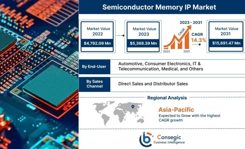
Semiconductor Memory IP Market size is estimated to reach over USD 15,691.47 Million by 2031 from a value of USD 4,792.09 Million in 2022 and is projected to grow by USD 5,368.39 Million in 2023, growing at a CAGR of 14.3% from 2023 to 2031.
Semiconductor Memory IP Market Major Driving Factors and Opportunities:
Several key factors are fueling the growth of the semiconductor memory IP market in 2025. Firstly, the relentless increase in the complexity and functionality of SoCs demands a wide variety of embedded memory solutions optimized for different performance, power, and area requirements. The proliferation of applications like AI, machine learning, high-performance computing (HPC), and advanced graphics processing units (GPUs) necessitates high-bandwidth and low-latency memory IP.
Secondly, the growing adoption of mobile devices, IoT gadgets, and connected vehicles is driving the demand for low-power and small-footprint memory IP solutions. Thirdly, the rising costs and complexities associated with designing and verifying advanced memory circuits in-house are making the licensing of pre-validated IP a more economically viable and technically sound option for semiconductor companies. This trend is particularly pronounced at advanced process nodes where design expertise is scarce and development costs are substantial.
The market also presents significant opportunities. The continuous evolution of non-volatile memory technologies, such as eMRAM, ReRAM, and FeRAM, which offer advantages in terms of speed, endurance, and power consumption compared to traditional Flash, is creating new opportunities for IP vendors. The increasing demand for secure memory solutions for applications like automotive and IoT is also driving innovation in memory IP with enhanced security features. Furthermore, the customization and optimization of memory IP for specific application requirements, such as AI inference at the edge, represent a growing area of opportunity. The development of memory IP compliant with emerging industry standards and interfaces also opens up new market segments.
Request Discount: https://www.consegicbusinessintelligence.com/request-discount/1323
Semiconductor Memory IP Market Scope:
The scope of the semiconductor memory IP market encompasses the licensing of various types of memory IP blocks for integration into SoCs. This includes:
SRAM IP: Offering high speed and low latency, used in cache memories, on-chip buffers, and register files. Different variations cater to specific speed and power requirements.
DRAM IP: Providing high density and lower cost per bit compared to SRAM, used as main memory in various electronic devices. This includes different generations like DDR5 and LPDDR5X.
ROM IP: For storing non-changeable data such as boot code and firmware. Various types like Mask ROM, OTP ROM, and EEPROM IP fall under this category.
Non-Volatile Memory (NVM) IP:
Flash IP: Widely used for persistent data storage in embedded systems and memory cards. Includes NOR and NAND Flash IP.
Emerging NVM IP (eMRAM, ReRAM, FeRAM): Offering potential advantages in terms of speed, power, and endurance, targeting applications requiring high performance and low power consumption.
Memory Controller IP: Intellectual property blocks that manage the interface and operation of embedded memory, ensuring efficient data access and control.
Memory Interface IP: IP that facilitates communication between the embedded memory and other components of the SoC, such as PHYs for high-speed DRAM interfaces.
The scope also includes the provision of associated services such as customization, integration support, and maintenance of the licensed IP. The market caters to a wide range of applications across various industries globally.
Buy Now: https://www.consegicbusinessintelligence.com/secure-checkout/1323
Semiconductor Memory IP Market Key Market Trends:
Several key trends are shaping the semiconductor memory IP market in 2025:
Focus on Low Power Consumption: With the proliferation of mobile and IoT devices, there is a strong demand for memory IP that minimizes power consumption while maintaining performance. This is driving innovation in low-voltage operation and power management features within memory IP blocks.
High Bandwidth Requirements: Applications like AI, HPC, and advanced graphics are demanding memory IP with increasingly higher bandwidth capabilities. This is leading to the adoption of advanced DRAM interfaces (e.g., DDR5, LPDDR5X) and specialized high-bandwidth memory (HBM) IP.
Integration of Security Features: Security is becoming a critical concern for embedded systems, particularly in automotive and IoT applications. Memory IP vendors are increasingly incorporating security features such as encryption, authentication, and physical unclonable functions (PUFs) into their designs.
Emergence and Adoption of New NVM Technologies: eMRAM, ReRAM, and FeRAM are gaining traction as alternatives to traditional Flash for embedded applications requiring high performance, low power, and high endurance. The availability of robust and reliable IP for these technologies is a key trend.
Customization and Optimization for Specific Applications: There is a growing trend towards tailoring memory IP solutions to meet the specific requirements of target applications, such as optimizing SRAM for AI accelerators or NVM for automotive reliability standards.
Advanced Process Node Compatibility: The demand for memory IP compatible with leading-edge process nodes (e.g., 3nm, 2nm) is increasing as semiconductor manufacturers strive for higher performance and density. IP vendors are investing heavily in developing and verifying their IP at these advanced nodes.
Chiplet-Based Architectures: The rise of chiplet-based designs, where different functional blocks of a system are implemented on separate dies and interconnected, is influencing the memory IP market. IP vendors are developing memory IP solutions that can be effectively integrated into such architectures.
Semiconductor Memory IP Market Key Players:
The semiconductor memory IP market in 2025 is characterized by a mix of established IP vendors and specialized companies. Some of the key players include:
Arm Limited
Rambus Inc.
eMemory Technology Inc.
Samsung
Micron Technology Inc.
Synopsys Inc.
Cadence Design Systems Inc.
SK Hynix Inc.
Dolphin Design SAS
Lattice Semiconductor
The competitive landscape is dynamic, with companies focusing on technological innovation, portfolio expansion, and strategic partnerships to gain market share.
Sample Report: https://www.consegicbusinessintelligence.com/request-sample/1323
Semiconductor Memory IP Market Segmentation:
The semiconductor memory IP market in 2025 can be segmented based on several factors:
By Sales Channel: Direct Sales and Distributor Sales
By End-User: Automotive, Consumer Electronics, IT & Telecommunication, Medical, and Others
Understanding these different segments is crucial for market analysis, identifying target markets, and developing effective business strategies.
Semiconductor Memory IP Market Opportunities and Challenges:
Opportunities:
Proliferation of Data-Intensive Applications: The increasing demand for processing and storing large amounts of data in AI, machine learning, and big data analytics is driving the need for high-performance memory IP.
Growth of Edge Computing: The rise of edge computing, where data processing occurs closer to the source, necessitates low-power and reliable embedded memory IP in a wide range of devices.
Stringent Requirements in Automotive Applications: The automotive industry’s increasing reliance on electronics, including ADAS and autonomous driving, demands high-reliability, high-performance, and secure memory IP.
Demand for Specialized Memory Solutions: Emerging applications are driving the need for specialized memory IP with unique characteristics, such as high endurance for data logging or low latency for real-time processing.
Increasing Complexity of SoC Designs: As SoCs become more complex, the value proposition of licensing pre-verified memory IP to reduce design risk and time-to-market becomes even more compelling.
Challenges:
High Development and Verification Costs: Developing and verifying memory IP at advanced process nodes is becoming increasingly expensive and complex.
Meeting Stringent Performance and Power Requirements: Balancing the demands for high performance and low power consumption in memory IP design is a significant technical challenge.
Ensuring Reliability and Yield at Advanced Nodes: Manufacturing memory at leading-edge nodes can present challenges in terms of reliability and yield, which can impact the value of the IP.
Integration Complexity: Integrating memory IP seamlessly into diverse SoC architectures and ensuring compatibility with other IP blocks can be complex.
Security Vulnerabilities: As memory IP becomes more integrated into critical systems, ensuring its security against various threats is paramount.
Competition and Pricing Pressures: The semiconductor IP market is competitive, and vendors face pressure to offer competitive pricing while maintaining profitability.
Semiconductor Memory IP Market Regional Analysis:
The semiconductor memory IP market in 2025 exhibits varying dynamics across different regions:
Asia Pacific: Expected to be the largest and fastest-growing market. The region is a major hub for semiconductor manufacturing and consumer electronics production, driving significant demand for memory IP. Countries like China, Taiwan, South Korea, and Japan are key contributors.
North America: A significant market driven by the presence of leading semiconductor design companies, particularly in the areas of high-performance computing, AI, and automotive.
Europe: A mature market with a strong focus on automotive, industrial, and telecommunications applications, driving demand for reliable and specialized memory IP.
Rest of the World: The market in other regions is growing at a steady pace, driven by increasing electronics adoption and the development of local semiconductor design capabilities.
Regional analysis helps to understand the specific application demands and growth opportunities in different parts of the world, allowing IP vendors to tailor their strategies accordingly.
Semiconductor Memory IP Market Recent Developments:
The semiconductor memory IP market as of April 2025 is characterized by several recent developments:
Continued Advancements in Emerging NVM IP: Significant progress is being made in the maturity and commercialization of eMRAM, ReRAM, and FeRAM IP, with increasing adoption in niche applications and ongoing efforts to scale them for broader use. Several IP vendors have announced new generations of these NVM IPs with improved performance and density.
Focus on AI and Machine Learning Optimization: Memory IP vendors are increasingly offering solutions specifically optimized for AI and machine learning workloads, including high-bandwidth SRAM and specialized embedded memory architectures.
Enhanced Security Features in Memory IP: New memory IP blocks are being introduced with advanced security features to address the growing concerns about data security in connected devices, particularly in automotive and IoT.
Development of IP for Chiplet Architectures: IP vendors are adapting their memory IP offerings to facilitate integration into chiplet-based designs, enabling greater flexibility and customization in SoC development.
Progress at Advanced Process Nodes: Several key IP vendors have announced the availability and successful tape-out of their memory IP at leading-edge process nodes like 3nm and 2nm, enabling the development of high-performance and power-efficient SoCs.
Strategic Collaborations and Partnerships: Collaborations between memory IP vendors, EDA companies, and foundries are increasing to ensure seamless integration and validation of memory IP in advanced semiconductor manufacturing processes.
Growing Emphasis on Low-Power Solutions: The demand for energy-efficient memory IP continues to drive innovation in low-voltage operation and power management techniques within memory IP designs.
Contact us:
Consegic Business intelligence Pvt Ltd.
B 202 , 2nd Floor, Ujwal Serene, Baner Road, Baner, Pune, Maharashtra – 411045.
Contact No: (US) (505) 715-4344
Email: sales@consegicbusinessintelligence.com
About Us: At Consegic Business Intelligence Pvt. Ltd., we empower businesses with actionable insights and innovative market intelligence solutions. Our tailored research and data-driven strategies help organizations navigate complex industry landscapes and make confident decisions.
Specializing in market research, consulting, and competitive analysis, we deliver precise and holistic insights across global and regional markets. Our client-focused approach ensures customized solutions that drive growth and foster informed decision-making.
This release was published on openPR.