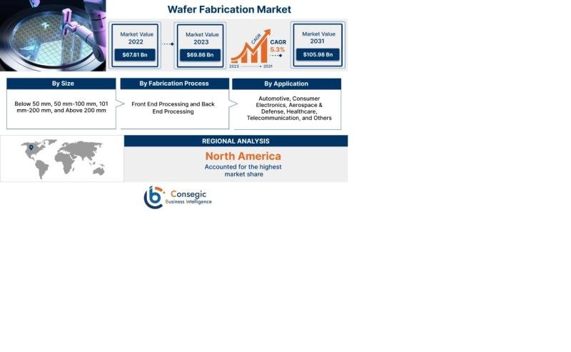
Wafer Fabrication Market
Wafer Fabrication Market Introduction:
The Wafer Fabrication Market encompasses the intricate processes involved in manufacturing semiconductor wafers, which are the foundational building blocks for integrated circuits (ICs) and other microelectronic components. These thin slices of semiconductor material, predominantly silicon, undergo a series of sophisticated steps to create the complex circuitry that powers modern electronics. The process typically begins with producing high-purity silicon ingots, which are then sliced into wafers of varying diameters (commonly 200mm and 300mm).
These wafers then undergo numerous processing stages within specialized fabrication facilities (fabs), including photolithography, etching, doping, deposition, and chemical-mechanical planarization. Each step is crucial for creating the layered structures and intricate patterns that define the functionality of semiconductor devices. Wafer fabrication is a highly precise and capital-intensive undertaking, demanding advanced equipment, specialized materials, and stringent quality control to ensure the performance and reliability of the final semiconductor products.
Get a sample report: https://www.consegicbusinessintelligence.com/request-sample/1369
Wafer Fabrication Market Major Driving Factors and Opportunities:
Several key factors are propelling the growth and evolution of the Wafer Fabrication Market. The increasing demand for electronics across various sectors, including consumer electronics (smartphones, laptops, wearables), automotive (electric vehicles, advanced driver-assistance systems), telecommunications (5G infrastructure), healthcare, and industrial automation, is a primary driver. This demand necessitates a higher production volume of semiconductor wafers to meet the growing need for integrated circuits.
Technological advancements in semiconductor manufacturing processes are also crucial. The continuous push towards smaller process nodes (e.g., 7nm, 5nm, and below) enables the production of more powerful and energy-efficient chips. Furthermore, the adoption of advanced materials like silicon carbide (SiC) and gallium nitride (GaN) for specialized applications, such as power electronics, is driving innovation in wafer fabrication techniques.
Emerging technologies like Artificial Intelligence (AI), the Internet of Things (IoT), and 5G networks are creating significant opportunities for the Wafer Fabrication Market. These technologies require advanced semiconductor devices with enhanced performance and integration capabilities, thus driving the demand for sophisticated wafer fabrication processes.
The expansion of renewable energy sources, particularly solar power, also contributes to the market growth, as silicon wafers are essential components in photovoltaic cells. Similarly, the growth of the electric vehicle (EV) market necessitates high-performance semiconductors for power management and control systems, further fueling the demand for wafer fabrication.
Request Discount: https://www.consegicbusinessintelligence.com/request-discount/1369
Wafer Fabrication Market Scope:
The scope of the Wafer Fabrication Market encompasses a wide range of activities and technologies involved in the production of semiconductor wafers. This includes the manufacturing of silicon ingots, the slicing and polishing of wafers, and the various wafer processing steps such as photolithography, etching, deposition, doping, and planarization. The market also includes the equipment used in these processes, such as lithography machines, etching equipment, deposition systems, and inspection tools. Furthermore, the scope extends to the materials consumed in wafer fabrication, including silicon, chemicals, gases, and photoresists.
The market can be segmented based on wafer size (e.g., 200mm, 300mm, and the future potential of 450mm), fabrication process (front-end-of-line for circuit creation and back-end-of-line for interconnection and packaging), node size (representing the minimum feature size on the chip, such as 7nm and below, 10nm, etc.), and end-user (foundries, memory manufacturers, integrated device manufacturers). Geographically, the market spans across regions with significant semiconductor manufacturing activities, including Asia Pacific, North America, and Europe. The scope also includes the ongoing research and development efforts focused on improving wafer quality, reducing manufacturing costs, and enabling the fabrication of more advanced semiconductor devices.
Buy Now: https://www.consegicbusinessintelligence.com/secure-checkout/1369
Key Market Trends:
While the primary focus is on the Wafer Fabrication Market, understanding the trends in the downstream Converter Modules Market provides valuable context, as the demand for these modules is intrinsically linked to the output of semiconductor wafers. Key trends in the Converter Modules
Market include:
Increasing demand for high-efficiency power conversion: Industries across various sectors are focusing on improving energy efficiency and reducing power losses, driving the need for highly efficient converter modules. This is particularly relevant in applications like renewable energy systems and electric vehicles.
Integration of wide-bandgap semiconductors: Materials like silicon carbide (SiC) and gallium nitride (GaN) are increasingly being adopted in converter modules due to their superior performance characteristics compared to silicon, such as higher efficiency, faster switching speeds, and better thermal conductivity.
Growing demand for modular and scalable solutions: There is a rising preference for converter modules that can be easily integrated into existing systems and scaled to meet varying power requirements, particularly in sectors like telecommunications and data centers.
Miniaturization and increased power density: The trend towards smaller and lighter electronic devices is driving the demand for compact converter modules with high power density without compromising performance, which is crucial in applications like aerospace and portable electronics.
Focus on digital power solutions: Digital control techniques are becoming more prevalent in converter modules, offering greater flexibility, programmability, and enhanced system management through real-time data analysis and remote diagnostics.
Development of application-specific modules: Manufacturers are increasingly focusing on creating converter modules tailored to the specific needs of high-growth applications such as electric vehicles, renewable energy systems, and industrial automation.
Advancements in packaging technologies: New packaging methods are being implemented to improve the reliability, durability, and thermal performance of converter modules, especially for harsh operating environments.
Get a sample report: https://www.consegicbusinessintelligence.com/request-sample/1369
Key Players:
The Wafer Fabrication Market is characterized by a mix of integrated device manufacturers (IDMs) that both design and manufacture chips, and foundries that specialize in manufacturing wafers for fabless semiconductor companies. Some of the key players in the Wafer Fabrication Market include:
Taiwan Semiconductor Manufacturing Company Limited
Tokyo Electron Limited
STMicroelectronics
SOITEC
Samsung
Intel Corporation
Lam Research Corporation
Motorola Solutions Inc.
Applied Materials Inc.
KLA Corporation
Other significant players include SK Hynix and Micron Technology, primarily known for memory chip fabrication, and materials suppliers like SUMCO Corporation, Siltronic AG, and GlobalWafers Co., Ltd. These companies consistently invest in research and development to advance process technologies, expand production capacities, and maintain their competitive edge in the rapidly evolving semiconductor landscape.
The Asia-Pacific region, particularly Taiwan, South Korea, and China, is home to many of these key players and plays a critical role in the global Wafer Fabrication Market.
Segmentation:
The Wafer Fabrication Market can be segmented in several ways to provide a more granular understanding of its dynamics:
By Size:
Below 50 mm
50 mm-100 mm
101 mm-200 mm
Above 200 mm
By Fabrication Process:
Front End Processing
Back End Processing
By Application:
Automotive
Consumer Electronics
Aerospace & Defense
Healthcare
Telecommunication
Others
By Region:
North America (U.S., Canada, Mexico)
Europe (Germany, France, UK, Italy, Rest of Europe)
Asia Pacific (China, Japan, South Korea, Taiwan, Rest of Asia Pacific)
Middle East & Africa
South America
These segmentations help in analyzing market trends, identifying growth opportunities, and understanding the specific demands of different parts of the Wafer Fabrication Market.
Wafer Fabrication Market Opportunities and Challenges:
The Wafer Fabrication Market presents numerous opportunities for growth and innovation:
Growth in AI, IoT, and 5G applications: These emerging technologies demand high-performance and specialized semiconductors, creating a need for advanced wafer fabrication capabilities.
Increasing demand for semiconductors in automotive electronics: The automotive industry’s shift towards electric vehicles and advanced driver-assistance systems requires sophisticated semiconductor solutions.
Expansion of renewable energy sector: The growing adoption of solar power increases the demand for silicon wafers used in photovoltaic cells.
Miniaturization and advanced packaging: The continuous trend towards smaller and more powerful electronic devices necessitates advancements in wafer fabrication and packaging technologies.
Sustainability and green manufacturing: There is a growing emphasis on developing environmentally friendly and sustainable wafer fabrication processes, offering opportunities for innovation in resource efficiency and waste reduction.
Government initiatives and investments: Many governments worldwide are investing in strengthening their domestic semiconductor manufacturing capabilities, creating favorable conditions for market growth.
However, the Wafer Fabrication Market also faces significant challenges:
High capital investment: Setting up and maintaining state-of-the-art fabrication facilities requires substantial financial resources, posing a barrier to entry for new players and requiring continuous investment for existing ones.
Technological complexity: Semiconductor manufacturing processes are highly complex and rapidly evolving, demanding continuous research and development and specialized expertise.
Miniaturization and scaling limitations: As feature sizes on wafers shrink, controlling critical dimensions and minimizing defects becomes increasingly challenging.
Material constraints: Traditional materials like silicon are approaching their physical and performance limits for certain advanced applications, necessitating the adoption of new materials which present their own manufacturing challenges.
Defect density: Maintaining low defect densities is crucial, especially with increasing wafer sizes, as defects can significantly impact yield and profitability.
Environmental impacts: Wafer fabrication consumes significant amounts of water and energy and produces hazardous waste, necessitating the development of more sustainable manufacturing practices.
Geopolitical tensions and supply chain disruptions: The semiconductor industry is vulnerable to geopolitical issues and trade disputes, which can impact the supply of raw materials and equipment.
Talent shortage: There is a growing need for highly skilled engineers and technicians with expertise in advanced semiconductor manufacturing processes.
Addressing these challenges through innovation, collaboration, and strategic investments will be crucial for the continued growth and success of the Wafer Fabrication Market.
Regional Analysis:
The Wafer Fabrication Market exhibits significant regional variations in terms of manufacturing capabilities, demand patterns, and growth drivers:
Asia Pacific: This region dominates the global Wafer Fabrication Market, with major manufacturing hubs in Taiwan, South Korea, China, and Japan. Taiwan, particularly through TSMC, holds the largest share of foundry capacity. South Korea is home to memory giants like Samsung and SK Hynix.
China is rapidly expanding its semiconductor manufacturing capabilities with strong government support. The high demand for consumer electronics and the presence of major electronics manufacturing industries in this region drive the market growth.
North America: The U.S. has a strong presence in semiconductor design and also has significant fabrication facilities, particularly for specialized chips. Government initiatives to boost domestic manufacturing are expected to further drive growth in this region. Canada and Mexico also contribute to the electronics manufacturing ecosystem.
Europe: Europe has a well-established semiconductor industry, focusing on specialized applications such as automotive and industrial electronics. Initiatives to strengthen the European semiconductor value chain are underway.
Rest of the World: The Middle East & Africa and South America have relatively smaller shares in the Wafer Fabrication Market but are witnessing increasing demand due to the growth of their electronics and automotive sectors. Investments in technology and infrastructure are expected to drive moderate growth in these regions.
The regional analysis highlights the concentration of advanced wafer fabrication capabilities in Asia Pacific, while other regions are focusing on strategic growth and self-sufficiency in semiconductor manufacturing. The ongoing geopolitical landscape is also influencing regional strategies and investments in the Wafer Fabrication Market.
Recent Developments:
Recent developments in the Converter Modules Market reflect the trends discussed earlier, with a strong emphasis on efficiency, integration, and new materials:
Introduction of converter modules utilizing GaN and SiC semiconductors: Several manufacturers have launched new product lines featuring wide-bandgap materials, offering higher efficiency and power density in smaller form factors.
Development of highly integrated digital power modules: Companies are releasing converter modules with integrated digital controllers, communication interfaces (e.g., PMBus), and advanced protection features for enhanced system management and monitoring.
Launch of application-specific converter modules: There is an increasing number of converter modules tailored for specific applications like electric vehicles (e.g., high-power DC-DC converters for auxiliary systems), renewable energy (e.g., DC-DC converters for solar inverters), and industrial automation.
Advancements in packaging technologies for improved thermal performance: Innovations in thermal management, such as advanced heat sinks and packaging materials, are enabling converter modules to operate reliably at higher power densities and in harsh environments.
Focus on miniaturization and higher power density: Manufacturers continue to innovate to reduce the size and weight of converter modules while increasing their power handling capabilities to meet the demands of space-constrained applications.
Development of bidirectional converters: Bidirectional DC-DC converters are gaining traction, particularly in applications like energy storage systems and electric vehicles, allowing power flow in both directions for efficient energy management.
Emphasis on sustainability and energy efficiency: There is a growing focus on developing converter modules with very high efficiency to minimize energy losses and reduce the overall environmental impact of electronic systems.
Contact us:
Consegic Business intelligence Pvt Ltd
B 202 , 2nd Floor, Ujwal Serene, Baner Road, Baner, Pune, Maharashtra – 411045.
(US) (505) 715-4344
info@consegicbusinessintelligence.com
About us:
At Consegic Business Intelligence Pvt. Ltd., we empower businesses with actionable insights and innovative market intelligence solutions. Our tailored research and data-driven strategies help organizations navigate complex industry landscapes and make confident decisions.
Specializing in market research, consulting, and competitive analysis, we deliver precise and holistic insights across global and regional markets. Our client-focused approach ensures customized solutions that drive growth and foster informed decision-making.
This release was published on openPR.