Chip Photomask Market
The chip photomask market is poised for steady expansion over the coming years as technological advancements and increasing semiconductor demands drive growth. This industry plays a crucial role in the fabrication of integrated circuits, and its evolution reflects broader trends in semiconductor manufacturing and innovation.
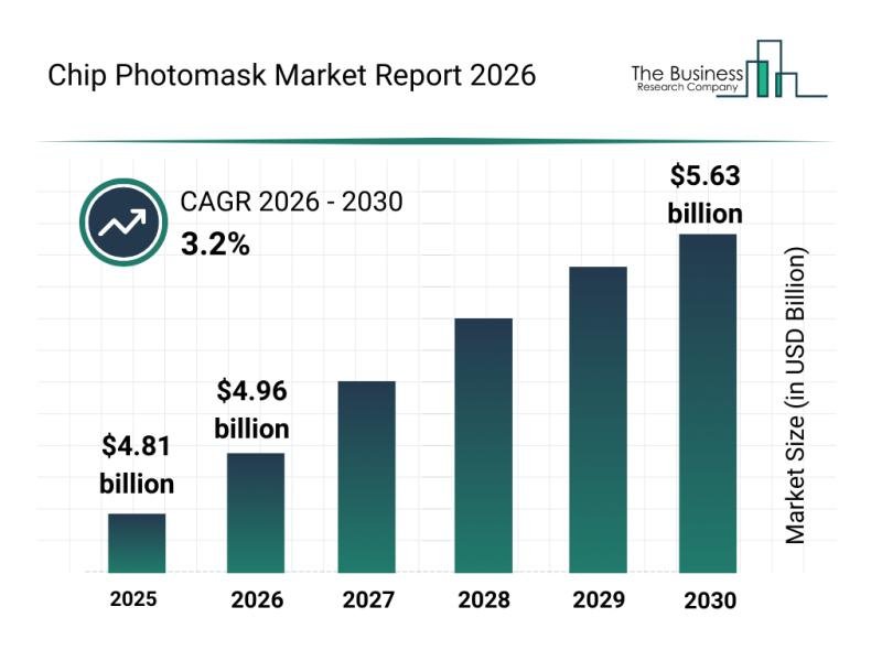
Projected Market Size and Growth Potential in the Chip Photomask Market
The chip photomask market is forecasted to reach a value of $5.63 billion by 2030, expanding at a compound annual growth rate (CAGR) of 3.2%. This anticipated growth is supported by several key factors, including the increasing use of extreme ultraviolet (EUV) photomasks, the rising complexity of integrated circuits (ICs), ongoing investments in smart manufacturing technologies, and the expansion of semiconductor foundries, particularly in North America and Europe. Additionally, breakthroughs in mask materials and coatings contribute significantly to market advancement. Key trends shaping this market include the miniaturization of IC components, adoption of advanced photolithography methods, precision mask manufacturing, widespread implementation of EUV and deep ultraviolet (DUV) lithography, and automation within semiconductor production lines.
Download a free sample of the chip photomask market report:
https://www.thebusinessresearchcompany.com/sample.aspx?id=21416&type=smp
Top Players Driving the Chip Photomask Industry Forward
Several prominent companies dominate the chip photomask market landscape. These include Applied Materials, ASML Holding N.V., DAI Nippon Printing Co. Ltd., Semiconductor Manufacturing International Corporation, Synopsys Inc., Hoya Corporation, Nikon Corporation, Benchmark Technologies, Hua Hong Semiconductor Limited, Photronics Inc., Lasertec Corporation, SUSS MicroTec, Taiwan Mask Corporation, Shenzhen Qingyi Photomask Limited, Laserlab, Inc., Heidelberg Instruments, HTA Photomask, Martin Photomask Services, Tekscend Photomask, and Mutech Microsystems. These firms lead innovation and supply, shaping the market’s future.
Strategic Collaborations Enhancing Capabilities in the Chip Photomask Market
Collaborations and partnerships are becoming increasingly important as companies seek to combine strengths and push technological boundaries. For example, in February 2025, US-based Toppan Photomask partnered with IBM to develop cutting-edge photomask technologies tailored for 2-nanometer (nm) logic semiconductor nodes and beyond. This collaboration focuses on utilizing extreme ultraviolet (EUV) lithography and High-NA EUV technology to advance photomask manufacturing capabilities. IBM, also headquartered in the US, is a key player in chip photomask production, and this alliance highlights the strategic nature of partnerships within the industry.
View the full chip photomask market report:
https://www.thebusinessresearchcompany.com/report/chip-photomask-global-market-report
Emerging Trends Highlighting Innovation and Efficiency in the Chip Photomask Market
Leading companies in the chip photomask sector are increasingly adopting strategic partnerships to accelerate the development of advanced chip technologies. Strategic partnerships involve cooperative agreements where companies share expertise and resources without losing their independence. A notable example is the November 2024 collaboration between Germany’s Tekscend Photomask Germany GmbH and the Advanced Mask Technology Center (AMTC). This partnership resulted in the launch of Europe’s first MBMW-100 Flex, a multibeam mask writer that drastically reduces mask writing time for intricate semiconductor designs-from several days down to just 7-12 hours. This advancement not only boosts efficiency but also strengthens Europe’s standing in the competitive semiconductor market.
Key Segments Defining the Chip Photomask Market Landscape
The global chip photomask market is divided into several critical segments to capture the full scope of the industry:
1) By Type: Binary Photomasks, Phase-Shifting Photomasks, Chromeless Photomasks, and Other Types
2) By Application: Semiconductor Manufacturing, Flat Panel Display Manufacturing, Micro-Electromechanical Systems (MEMS), and Other Applications
3) By End-Use Industry: Consumer Electronics, Automotive, Telecommunications, and Healthcare
Detailed subcategories include:
– Binary Photomasks: Conventional Binary, Optical Enhancements, High-Resolution, and Deep UV (DUV) Binary Photomasks
– Phase-Shifting Photomasks: Alternating Phase-Shifting (Alt-PSM), Attenuated Phase-Shifting (Att-PSM), Rim-Shifting, and Sub-Wavelength Phase-Shifting Variants
– Chromeless Photomasks: Scattering-Based, Interference-Based, Advanced Lithography, and Extreme UV (EUV) Chromeless Types
– Other Types: Extreme Ultraviolet (EUV) Photomasks, Nano-Imprint Lithography Photomasks, Multi-Layer Mask Photomasks, and Hybrid Photomasks
This segmentation provides a comprehensive framework for analyzing the diverse applications and technologies within the chip photomask market.
Reach out to us:
The Business Research Company: https://www.thebusinessresearchcompany.com/,
Americas +1 310-496-7795,
Europe +44 7882 955267,
Asia & Others +44 7882 955267 & +91 8897263534,
Email us at info@tbrc.info.
Follow Us On:
LinkedIn: https://in.linkedin.com/company/the-business-research-company,
Twitter: https://twitter.com/tbrc_info,
YouTube: https://www.youtube.com/channel/UC24_fI0rV8cR5DxlCpgmyFQ
Learn More About The Business Research Company
With over 17500+ reports from 27 industries covering 60+ geographies, The Business Research Company has built a reputation for offering comprehensive, data-rich research and insights. Armed with 1,500,000 datasets, the optimistic contribution of in-depth secondary research, and unique insights from industry leaders, you can get the information you need to stay ahead.Our flagship product, the Global Market Model (GMM), is a premier market intelligence platform delivering comprehensive and updated forecasts to support informed decision-making.
This release was published on openPR.