GaN Substrate Market
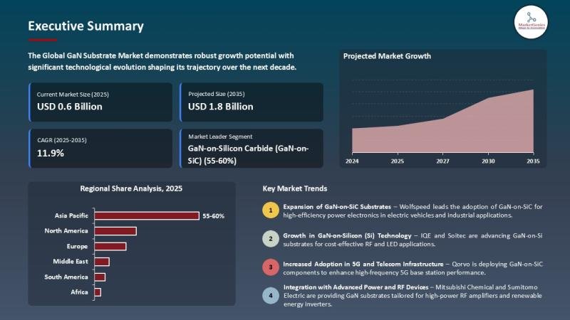
According to the report, the global GaN substrate market is likely to grow from USD 0.6 Billion in 2025 to USD 1.8 Billion in 2035 at a highest CAGR of 11.9% during the time period. Global GaN substrate market is observing high growth rates as a result of semiconductor advancement and the growing need of high-performance electronic devices. The development of technologies in the fabrication of wafer has allowed manufacturing of bigger diameter substrates with improvement of yield including 6-inch and 8-inch diameter wafers with lower manufacturing cost.
Moreover, the growing tendency towards electric cars (EVs) and renewable energy solutions has led to the increase in the need of high-efficiency power devices, and in this case, the use of GaN substrates is essential. Firms such as Infineon Technologies are currently working on the GaN technology in order to meet this increased demand, focusing on the efficiency and reliability of their power semiconductor products. The mentioned developments have highlighted the critical importance of GaN substrates in enhancing power electronics and facilitating the shift towards more sustainable energy systems.
Get the Detailed Industry Analysis (including the Table of Contents, List of Figures, and List of Tables) – from the GaN Substrate Market Research Report: https://marketgenics.co/press-releases/gan-substrate-market-96029
Regional Analysis of Global GaN Substrate Market
The GaN substrates demand is largest in Asia Pacific because the region is experiencing high growth in EV production, renewable energy systems and 5G systems. In June 2025, Mitsubishi Electric moved to the next stage of manufacturing GaN-on-SiC wafers in Japan, which would target high-efficiency inverters in industrial and automotive markets, which proves the technological competence and maturity of the supply chains in the region. The high penetration of GaN substrates is in Asia Pacific because of the scale of its manufacturing and increasing high-performance electronics demand in the region.
The North America region is also experiencing high growth due to strong semiconductor R&D infrastructure and early adoption of GaN for defense and aerospace applications. Wolfspeed’s expanded North Carolina facility for GaN-on-SiC wafers highlights growing production capacity.
Prominent players operating in the global GaN substrate market are DOWA Electronics Materials, Enkris Semiconductor, EpiGaN (Soitec subsidiary), Eta Research, GLC Semiconductor Group, IQE plc, Kyma Technologies, LumiGNtech co., Ltd., Mitsubishi Chemical Corporation, MSE Supplies LLC, Nanowin Technology, Nitride Semiconductors Co., Ltd., PAM-XIAMEN, Qorvo, Saint-Gobain, Sciocs Company Limited, Semiconductor Wafer Inc., Sino Nitride Semiconductor, Soitec, Sumitomo Electric Industries, Ltd., Suzhou Nanowin Science and Technology, Wolfspeed, Inc., Xiamen Powerway Advanced Material Co., Ltd., and Other Key Players.
To know more about the GaN Substrate Market – Download our Sample Report: https://marketgenics.co/download-report-sample/gan-substrate-market-96029
Key Driver, Restraint, and Growth Opportunity Shaping the Global GaN Substrate Market
The growing adoption of GaN substrates in high frequency radar and satellite communications systems joins the demand in the market since the systems need high levels of thermal stability and efficiency. As an example, Northup Grumman used GaN-on-SiC wafers to create superior defence radar chipsets to improve signal strength and reliability.
Minimal supply of quality and defect free GaN wafers still serves as a constraint to the growth of the market because manufacturing issues related to up-scaling of wafer size may lead to higher costs of production. Even major competitors such as Sumitomo Chemical are yielding losses in trying to use larger diameter substrates in power devices.
The new usage of GaN substrates in data center power electronics has a high potential of growth given that high efficiency and high-density power conversion are required. Efforts of Infineon Technologies in making server power supplies using GaN-on-SiC technology are just some examples of how such an application can increase markets beyond auto and RF industries.
Buy Now: https://marketgenics.co/buy/gan-substrate-market-96029
Recent Development and Strategic Overview:
In July 2025, Incize ND Atomera, announced a strategic collaboration to enhance Gallium Nitride on Silicon (GaN-on-Si) technologies. The joint program will concentrate on optimizing GaN-on-Si device performance for high-frequency and high-power applications, with target markets in wireless infrastructure (5G/6G), satellite communications and advanced power electronics.
In June 2025, Sumitomo Electric and Osaka Metropolitan University successfully fabricated a GaN-HEMT on a 2-inch polycrystalline diamond (PCD) substrate in a joint research project with the Japan Science and Technology Agency (JST). The GaN layer used in this study was provided by Air Water as a GaN/SiC epitaxial layer on a silicon substrate.
Get a preview of our GaN Substrate Market Playbook – your guide to GTM strategy, competitive intelligence, supplier dynamics, and Consumer Behavior Analysis: https://marketgenics.co/playbook/gan-substrate-market-96029
Key Trend: Industry Consolidation Through Strategic Vertical Integration Reshaping Competitive Market Dynamics
With several of the largest manufacturers of semiconductor devices exploring vertical integration business models, the gallium nitrate substrate business is undergoing a dramatic structural change, with large-scale manufacturers buying the specialized substrate manufacturers to ensure supply chains and in the process capture the value of the whole manufacturing ecosystem. The strategic significance of this trend of consolidation is shown by the need to control substrate production capacity as downstream uses grow and allow integrated manufacturers to streamline the epitaxial processes, decrease interdependencies, and shorten the product development cycles.
The larger companies understand that the proprietary substrate technology offers a competitive edge in device markets that are becoming more commoditized, and that mergers and acquisitions across the entire value chain are aggressively pursued. Coherent Corp also acquired Japan-based bulk Grower of GaN substrates Sciocs Company in November 2024, and combined bulk growth of the crystal with its existing portfolio of Compound semiconductor to achieve a vertical integration of substrate manufacturing to final device manufacturing.
This acquisition is indicative of the strategic transformation of the industry toward consolidated business models that remove weak points in the supply chain and allow closer control over the product quality, costs of production and the technological innovation paths.
Contact:
Mr. Debashish Roy
MarketGenics India Pvt. Ltd.
800 N King Street, Suite 304 #4208, Wilmington, DE 19801, United States
USA: +1 (302) 303-2617
Email: sales@marketgenics.co
Website: https://marketgenics.co
About Us
MarketGenics is a global market research and management consulting company empowering decision makers across healthcare, technology, and policy domains. Our mission is to deliver granular market intelligence combined with strategic foresight to accelerate sustainable growth.
We support clients across strategy development, product innovation, healthcare infrastructure, and digital transformation.
This release was published on openPR.