Advanced Semiconductor Packaging Market
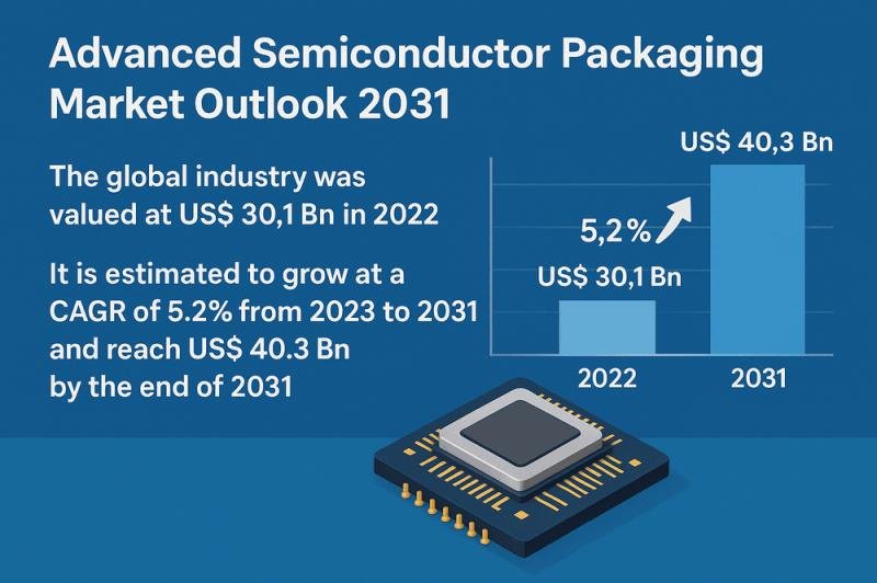
According to a new report, the Global Advanced Semiconductor Packaging Market was valued at USD 30.1 billion in 2022 and is projected to grow at a CAGR of 5.2% between 2023 and 2031, reaching USD 40.3 billion by the end of 2031. This robust expansion is being driven by the proliferation of consumer electronics, the miniaturization of devices, and ongoing innovations in wafer‐level and flip‐chip packaging technologies.
Explore core findings and critical insights from our Report in this sample – https://www.transparencymarketresearch.com/sample/sample.php?flag=S&rep_id=15743
Market Overview
Advanced semiconductor packaging encompasses a variety of techniques Fan‐Out Wafer‐Level Packaging (FOWLP), Fan‐In Wafer‐Level Packaging (FIWLP), Flip Chip (FC), and 2.5D/3D packaging designed to provide higher input/output (I/O) density, superior electrical performance, and reduced form factors compared to traditional packaging. Key end markets include consumer electronics, computing (CPUs/GPUs), telecommunications, automotive, aerospace, medical devices, and industrial applications. The shift toward more integrated, multi‐die configurations and greater emphasis on thermal management has further fueled demand for these cutting‐edge solutions.
Market Drivers & Trends
Surging Consumer Electronics Adoption: Global spending on wearables reached an estimated US$ 52 billion in 2020 (27% year‐over‐year growth), reflecting end‐user appetite for smartwatches, fitness trackers, and AR/VR headsets.
Proliferation of IoT Devices: As homes and industries deploy smart sensors and actuators, demand for compact, high‐performance packaging has intensified, pushing vendors to innovate in security‐hardened wafer‐level solutions.
Wafer‐Level Packaging Focus: R&D spending is increasingly allocated to FOWLP, which supports multiple dies in a single package and allows for thinner form factors versus FIWLP. Larger wafer diameters (e.g., 300 mm and emerging 450 mm) are being adopted to increase throughput and drive economies of scale.
Flip Chip Momentum: In 2022, flip chip held the largest share of the packaging‐type segment, thanks to its low profile, high I/O density, and superior signal integrity critical for high‐speed computing and mobile applications.
Key Players and Industry Leaders
The advanced semiconductor packaging landscape is highly competitive, with a mix of integrated device manufacturers (IDMs) and outsourced semiconductor assembly and test (OSAT) providers:
Advanced Micro Devices, Inc.
Intel Corporation
Amkor Technology
STMicroelectronics
Hitachi, Ltd.
Infineon Technologies AG
Avery Dennison Corporation
Sumitomo Chemical Co., Ltd.
ASE Technology Holding Co., Ltd.
KYOCERA Corporation
These organizations are enhancing their portfolios via strategic investments in packaging and test facilities, partnerships with foundries, and targeted R&D to develop next‐generation materials and processes.
Recent Developments
November 2023 – Amkor Technology announced a US$ 2.0 billion investment to build a new advanced packaging and test facility in Arizona to support packaging of Apple Inc. chips manufactured at nearby TSMC foundries.
November 2023 – Resonac (formerly JSR Corporation) unveiled plans for a Silicon Valley R&D center dedicated to advanced packaging materials, focusing on underfill resins and high‐reliability substrates.
Latest Market Trends
Heterogeneous Integration: Combining logic, memory, and analog dies in 2.5D/3D stacks is accelerating, driven by AI, HPC, and 5G base station requirements.
Eco‐Friendly Packaging: Biodegradable and low‐toxicity underfills and mold compounds are gaining attention amidst tightening environmental regulations.
Embedded Die Technologies: Embedding active dies within substrate layers is emerging as a path to greater miniaturization and improved thermal characteristics.
Market Opportunities
Automotive Electrification: Advanced driver‐assistance systems (ADAS), infotainment, and electric‐vehicle power electronics demand high‐reliability, temperature‐tolerant packaging solutions.
5G and Beyond: Millimeter‐wave modules for 5G infrastructure and user equipment require sophisticated packaging to maintain signal integrity at higher frequencies.
Medical Devices: Implantable and wearable medical electronics benefit from ultra‐compact, biocompatible packaging technologies.
Future Outlook
The advanced packaging market is poised to evolve toward even finer interconnect pitches and greater integration densities. Emerging trends include:
Chiplet Ecosystems: Standardized interfaces enabling modular assembly of heterogeneous chiplets.
Optical Interconnects: Integration of photonic links for ultra‐high bandwidth and low latency in data centers and HPC.
AI‐Driven Process Control: Machine‐learning algorithms optimizing yield and throughput in packaging lines.
Buy this Premium Research Report to explore detailed market trends – https://www.transparencymarketresearch.com/checkout.php?rep_id=15743<ype=S
Market Segmentation
By Packaging Type
Fan‐Out Wafer‐Level Packaging (FOWLP)
Fan‐In Wafer‐Level Packaging (FIWLP)
Flip Chip
2.5D/3D Packaging
By Application
Processor/Baseband
Central Processing Units/Graphical Processing Units (CPUs/GPUs)
Dynamic Random Access Memory (DRAM)
NAND Flash
Image Sensors
Others
By End‐User
Telecommunications
Automotive
Aerospace & Defense
Medical Devices
Consumer Electronics
Others
Regional Insights
Asia Pacific dominated in 2022, driven by China, Taiwan, South Korea, and India. India’s consumer electronics market was valued at US$ 13.8 billion in 2020 and is forecast to grow at a CAGR of 14.5% from 2021 to 2026. Smartphone shipments hit 150 million units in 2020, making India the world’s second‐largest smartphone market after China.
North America benefits from strong R&D hubs in the U.S. and leading fabless/OSAT players.
Europe is leveraging automotive and industrial demand, with Germany, France, and the U.K. as key markets.
Middle East & Africa and South America are emerging markets, with growth in telecom infrastructure investments.
Frequently Asked Questions
What is advanced semiconductor packaging?
Advanced packaging refers to methods such as FOWLP, FIWLP, flip chip, and 2.5D/3D-designed to increase I/O density, improve electrical/thermal performance, and reduce package size versus traditional wire‐bonded packages.
What factors are driving market growth?
Key drivers include the growing demand for wearables, smartphones, IoT devices, data‐center expansion, and automotive electrification, all of which require high‐performance, compact packaging solutions.
Which regions offer the best growth prospects?
Asia Pacific leads today, with strong electronics manufacturing and end‐market demand in China, Taiwan, South Korea, and India. North America and Europe are also poised for growth, driven by R&D and automotive/industrial applications.
Who are the major vendors?
Prominent players include AMD, Intel, Amkor Technology, STMicroelectronics, Hitachi, Infineon, Avery Dennison, Sumitomo Chemical, ASE Technology, and KYOCERA. Their strategic initiatives-facility expansions, R&D investments, and partnerships shape competitive dynamics.
How will emerging technologies impact the market?
Heterogeneous integration (chiplets), optical interconnects, and AI‐driven process controls are expected to redefine performance benchmarks, enabling even greater miniaturization and efficiency in the next generation of electronic systems.
Explore Latest Research Reports by Transparency Market Research:
Next-generation Solar Cell Market: https://www.transparencymarketresearch.com/next-generation-solar-cell-market.html
Small-caliber Ammunition Market: https://www.transparencymarketresearch.com/small-caliber-ammunition-market.html
RF Chip Inductor Market: https://www.transparencymarketresearch.com/rf-chip-inductor-market.html
Photonic Integrated Circuits (PIC) Market: https://www.transparencymarketresearch.com/photonic-integrated-circuit.html
About Transparency Market Research
Transparency Market Research, a global market research company registered at Wilmington, Delaware, United States, provides custom research and consulting services. Our exclusive blend of quantitative forecasting and trends analysis provides forward-looking insights for thousands of decision makers. Our experienced team of Analysts, Researchers, and Consultants use proprietary data sources and various tools & techniques to gather and analyses information.
Our data repository is continuously updated and revised by a team of research experts, so that it always reflects the latest trends and information. With a broad research and analysis capability, Transparency Market Research employs rigorous primary and secondary research techniques in developing distinctive data sets and research material for business reports.
Contact:
Transparency Market Research Inc.
CORPORATE HEADQUARTER DOWNTOWN,
1000 N. West Street,
Suite 1200, Wilmington, Delaware 19801 USA
Tel: +1-518-618-1030
USA – Canada Toll Free: 866-552-3453
Website: https://www.transparencymarketresearch.com
Email: sales@transparencymarketresearch.com
This release was published on openPR.