Semiconductor Metrology And Inspection
The Semiconductor Metrology And Inspection Market Report by The Business Research Company delivers a detailed market assessment, covering size projections from 2025 to 2034. This report explores crucial market trends, major drivers and market segmentation by [key segment categories].
What Is the Semiconductor Metrology And Inspection Market Size and Projected Growth Rate?
The size of the semiconductor metrology and inspection market has seen robust growth recently. The market’s worth is predicted to expand from $7.99 billion in 2024 to $8.46 billion in 2025, representing a compound annual growth rate (CAGR) of 5.9%. Factors contributing to this growth throughout the historic period include the downsizing of semiconductor devices, an escalating demand for improved semiconductor yields, demanding quality benchmarks, the need for better process controls, endeavours to decrease defects, the global expansion of semiconductor production, and the rise in wafer sizes.
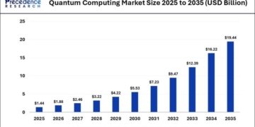
Predictions showcase a promising increase in the semiconductor metrology and inspection market in the coming years, escalating to an estimated $11.13 billion in 2029 with a compound annual growth rate (CAGR) seated at a sturdy 7.1%. Factors such as the amplified intricacy of semiconductor designs, the incorporation of metrology in developing processes, a dedicated focus on intelligent manufacturing, the initiation of EUV lithography, sustainable and environmental factors, and the development of foundries and outsourced semiconductor manufacturing are all propelling this growth. Notable trends forecasted to emerge during this period include breakthroughs in process technology, 3D integration and packaging, multi-modal metrology, in-line process management, advanced inspection of materials, the rise of nanotechnology and miniaturization, progressive defect inspection, and metrology’s role in quantum computing.
Purchase the full report for exclusive industry analysis:
https://www.thebusinessresearchcompany.com/purchaseoptions.aspx?id=8529
What Are the Major Segments in the Semiconductor Metrology And Inspection Market?
The semiconductor metrology and inspection market covered in this report is segmented –
1) By Type: Optical, E-Beam
2) By Lithography Metrology: Overlay, Dimension Equipment, Mask Inspection And Metrology
3) By Application: Lithography Metrology, Wafer Inspection, Thin Film Metrology
Subsegments:
1) By Optical: Optical Inspection Systems, Scatterometry, Interferometry, Reflective Measurement Systems
2) By E-Beam: E-Beam Inspection Systems, E-Beam Metrology Systems, E-Beam Lithography Tools
Get your free sample here:
https://www.thebusinessresearchcompany.com/sample.aspx?id=8529&type=smp
What Are The Driving Semiconductor Metrology And Inspection Market Evolution?
The surge in the usage of smart devices is fueling the semiconductor metrology and inspection market’s growth. A smart device refers to any gadget that features a wireless connection and can link to an app, the internet, a local network, or even another device. This rise in smart device usage is attributed to enhanced user experiences, growing recognition of the benefits of smart device technology, and the expanding number of dependable internet connections. The semiconductor metrology and inspection processes are vital for smart devices to ensure that every stage of semiconductor production is carried out to the highest possible standard. As an example, a Cybercrew report from March 2023 – a UK firm that creates and offers cybersecurity solutions for businesses of all sizes – highlighted that 91.43% of UK households used smartphones in 2021. This figure is expected to rise to 93.8% in 2026. Therefore, the increasing application of smart devices is set to boost the semiconductor metrology and inspection market.
Which Firms Dominate The Semiconductor Metrology And Inspection Market Segments?
Major companies operating in the semiconductor metrology and inspection market are KLA Corporation, Applied Materials Inc., Onto Innovation Inc. (Rudolph Technologies Corporation), Thermo Fisher Scientific Inc., Hitachi High-Tech Corporation, Nova Measuring Instruments Ltd., ASML Holding NV, Lasertec Corporation, JEOL Ltd., Nikon Metrology NV, Camtek Limited, Bruker Corporation, Nanometrics Incorporated, Horiba Ltd., Carl Zeiss AG, SENTECH Instruments GmbH, Keyence Corporation, Accurion GmbH, Alicona Imaging GmbH, Angstrom Engineering Inc., Nanofilm Technologies Inc, Veeco Instruments Inc., FormFactor Inc., Lam Research Corporation, INFICON Holding AG
What Trends Are Expected to Dominate the Semiconductor Metrology And Inspection Market in the Next 5 Years?
The accelerating trend in the semiconductor metrology and inspection market is product innovation. Key players in this market are prioritizing the invention of new technologies to enhance the inspection process and guarantee the quality of semiconductor devices. For instance, Onto Innovation, a US semiconductor manufacturer, unveiled innovative acoustic metrology products in July 2022. These included the new Echo system, expanding the market for in-line characterization of opaque films. Covering a broad spectrum of film thicknesses, from ultra-thin 50 films to 35m opaque films and metal layers, the Echo system operates at three times the signal-to-noise ratio (SNR) of earlier systems. In addition, the Echo system provides thermal conductivity measurement and in-line time domain thermo-reflectance for implant monitoring.
Get the full report for exclusive industry analysis:
https://www.thebusinessresearchcompany.com/report/semiconductor-metrology-and-inspection-global-market-report
Which Is The Largest Region In The Semiconductor Metrology And Inspection Market?
Asia-Pacific was the largest region in the semiconductor metrology and inspection market in 2024. Asia-Pacific is expected to be the fastest-growing region in the forecast period. The regions covered in the semiconductor metrology and inspection market report are Asia-Pacific, Western Europe, Eastern Europe, North America, South America, Middle East, Africa.
Frequently Asked Questions:
1. What Is the Market Size and Growth Rate of the Semiconductor Metrology And Inspection Market?
2. What is the CAGR expected in the Semiconductor Metrology And Inspection Market?
3. What Are the Key Innovations Transforming the Semiconductor Metrology And Inspection Industry?
4. Which Region Is Leading the Semiconductor Metrology And Inspection Market?
Why This Report Matters:
Competitive overview: This report analyzes the competitive landscape of the 3D imaging software market, evaluating key players on market share, revenue, and growth factors.
Informed Decisions: Understand key strategies related to products, segmentation, and industry trends.
Efficient Research: Quickly identify market growth, leading players, and major segments.
Connect with us on:
LinkedIn: https://in.linkedin.com/company/the-business-research-company,
Twitter: https://twitter.com/tbrc_info,
YouTube: https://www.youtube.com/channel/UC24_fI0rV8cR5DxlCpgmyFQ.
Contact Us
Europe: +44 207 1930 708,
Asia: +91 88972 63534,
Americas: +1 315 623 0293 or
Email: mailto:info@tbrc.info
Learn More About The Business Research Company
With over 15,000+ reports from 27 industries covering 60+ geographies, The Business Research Company has built a reputation for offering comprehensive, data-rich research and insights. Our flagship product, the Global Market Model delivers comprehensive and updated forecasts to support informed decision-making.
This release was published on openPR.